Science and Technology Foresight ›› 2022, Vol. 1 ›› Issue (3): 20-41.DOI: 10.3981/j.issn.2097-0781.2022.03.002
• Review and Commentary • Previous Articles Next Articles
BU Weihai1,†( ), XIA Zhiliang2, ZHAO Zhiguo1, LIU Yun1, ZHOU Yikang1
Received:2022-07-31
Revised:2022-09-01
Online:2022-09-20
Published:2022-11-04
Contact:
BU Weihai
卜伟海1,†(), 夏志良2, 赵治国1, 刘芸1, 周亦康1
通讯作者:
卜伟海
作者简介:卜伟海,教授级高级工程师。现任北方集成电路技术创新中心副总经理、技术开发与合作负责人。主要研究方向为先进逻辑器件与工艺、嵌入式新型存储技术等。曾作为国内领先集成电路企业的先导技术研发团队骨干和负责人完成多个节点工艺技术预研,主持和参与国家“863”计划、国家重点研发计划、国家科技重大专项02专项等多个重大项目。入选北京市优秀人才培养资助计划、北京经济技术开发区“亦麒麟”杰出人才。合作撰写专著2部,发表论文20余篇,获授权发明专利52项。电子信箱: weihai_bu@sticbj.com。
BU Weihai, XIA Zhiliang, ZHAO Zhiguo, LIU Yun, ZHOU Yikang. Development of Integrated Circuit Industrial Technologies in the Post-Moore Era[J]. Science and Technology Foresight, 2022, 1(3): 20-41.
卜伟海, 夏志良, 赵治国, 刘芸, 周亦康. 后摩尔时代集成电路产业技术的发展趋势[J]. 前瞻科技, 2022, 1(3): 20-41.
Add to citation manager EndNote|Ris|BibTeX
URL: http://www.qianzhankeji.cn/EN/10.3981/j.issn.2097-0781.2022.03.002


| 工艺类型 | 芯片与芯片 | 芯片与晶圆 | 晶圆与晶圆 |
|---|---|---|---|
| 示意图 |  |  |  |
| 优势 | 工艺灵活,采用合格芯粒,良率高 | 易于集成混合键合工艺; 工艺灵活,采用合格芯粒,良率高 | 成本低; 生产效率高 |
| 劣势 | 不利于规模化生产; 不易加工和键合; 静电阻抗器要求高 | 静电阻抗器要求高; 不易加工和键合 | 混合键合工艺集成困难; 良率不易保障 |
| 工艺类型 | 芯片与芯片 | 芯片与晶圆 | 晶圆与晶圆 |
|---|---|---|---|
| 示意图 | | | |
| 优势 | 工艺灵活,采用合格芯粒,良率高 | 易于集成混合键合工艺; 工艺灵活,采用合格芯粒,良率高 | 成本低; 生产效率高 |
| 劣势 | 不利于规模化生产; 不易加工和键合; 静电阻抗器要求高 | 静电阻抗器要求高; 不易加工和键合 | 混合键合工艺集成困难; 良率不易保障 |
| [1] | 卜伟海, 唐粕人. 后摩尔定律时代的工艺[M]// 王阳元. 集成电路产业全书(中册). 北京: 电子工业出版社, 2018. |
| [2] | IEEE. International roadmap for devices and systems more moore (2021 update)[EB/OL]. [2022-07-17]. https://irds.ieee.org/editions/2021/more-moore. |
| [3] | 卜伟海. 鳍式场效应晶体管[M]// 王阳元. 集成电路产业全书(中册). 北京: 电子工业出版社, 2018. |
| [4] | Cai J. CMOS device technology for the next decade[R]. 2021 Symposia on VLSI Technology and Circuits, 2021: SC1-1. |
| [5] | 武咏琴, 卜伟海, 康劲, 等. 3 nm以下技术代FinFET及围栅器件的发展与挑战[J]. 微纳电子与智能制造, 2021, 3(1): 14-26. |
| [6] |
Razavieh A, Zeitzoff P, Brown D E, et al. Scaling challenges of FinFET architecture below 40 nm contacted gate pitch[C]// 2017 75th Annual Device Research Conference. Piscataway: IEEE Press, 2017, doi: 10.1109/DRC.2017.7999495.
DOI |
| [7] | Cheng K, Parck C, Wu H, et al. Improved air spacer for highly scaled CMOS technology[J]. IEEE Transaction on Election Devices, 2020, 67(12): 5355-5361. |
| [8] |
Yeap G, Lin S S, Chen Y M, et al. 5 nm CMOS production technology platform featuring full-fledged EUV, and high mobility channel FinFETs with densest 0.021 µm2 SRAM cells for mobile SoC and high performance computing applications[C]// 2019 IEEE International Electron Devices Meeting. Piscataway: IEEE Press, 2020, doi: 10.1109/IEDM19573.2019.8993577.
DOI |
| [9] | 3 nm technology[EB/OL]. [2022-07-09]. https://www.tsmc.com/japanese/dedicatedFoundry/technology/logic/l_3nm. |
| [10] | Horiguchi N. Nanosheet device architectures to enable CMOS scaling in 3 nm and beyond: Nanosheet, Forksheet and CFET: The short course of 2021 Symposia on VLSI Technology and Circuits[R]. 2021: SC1-2. |
| [11] | SMIC 7 nm technology found in MinerVa bitcoin miner[EB/OL]. [2022-09-01]. https://www.techinsights.com/blog/disruptive-technology-7nm-smic-minerva-bitcoin-miner. |
| [12] | Lin C H. Beyond FinFET devices: GAA, CFET, and 2D material FET: The short course of 2021 International Electron Devices Meeting[R]. 2021: SC1-4. |
| [13] |
Barraud S, Previtali B, Vizioz C, et al. 7-levels-stacked nanosheet GAA transistors for high performance computing[C]// 2020 IEEE Symposium on VLSI Technology. Piscataway: IEEE Press, 2020, doi: 10.1109/VLSITechnology18217.2020.9265025.
DOI |
| [14] | Bardon M Garcia, Sherazi Y, Jang D, et al. Power-performance trade-offs for lateral nanosheets on ultra-scaled standard cells[C]// 2018 IEEE Symposium on VLSI Technology. Piscataway: IEEE Press, 2018: 143-144. |
| [15] |
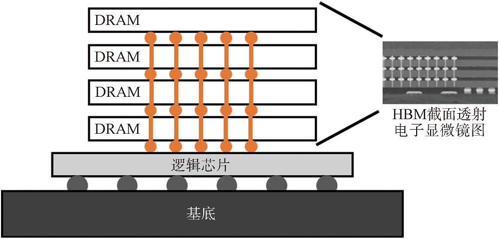
Bao R, Watanabe K, Zhang J, et al. Selective enablement of dual dipoles for near bandedge multi-Vt solution in high performance FinFET and nanosheet technologies[C]// 2020 IEEE Symposium on VLSI Technology. Piscataway: IEEE Press, 2020, doi: 10.1109/VLSITechnology18217.2020.9265010.
DOI |
| [16] |
Zhang J, Frougier J, Greene A, et al. Full bottom dielectric isolation to enable stacked nanosheet transistor for low power and high performance applications[C]// 2019 IEEE International Electron Devices Meeting. Piscataway: IEEE Press, 2020, doi: 10.1109/IEDM19573.2019.8993490.
DOI |
| [17] |
Mochizuki S, Bhuiyan M, Zhou H, et al. Stacked gate-all-around nanosheet pFET with highly compressive strained Si1-xGex channel[C]// 2020 IEEE International Electron Devices Meeting. Piscataway: IEEE Press, 2021, doi: 10.1109/IEDM13553.2020.9372041.
DOI |
| [18] |
Agrawal A, Chouksey S, Rachmady W, et al. Gate-all-around strained Si0.4Ge0.6 nanosheet PMOS on strain relaxed buffer for high performance low power logic application[C]// 2020 IEEE International Electron Devices Meeting. Piscataway: IEEE Press, 2021, doi: 10.1109/IEDM13553.2020.9371933.
DOI |
| [19] | Tian Y, Huang R, Wang Y, et al. New self-aligned silicon nanowire transistors on bulk substrate fabricated by epi-free compatible CMOS technology: Process integration, experimental characterization of carrier transport and low frequency noise[C]// 2007 IEEE International Electron Devices Meeting. Piscataway: IEEE Press, 2008: 895-898. |
| [20] |
Weckx P, Ryckaert J, Putcha V, et al. Stacked nanosheet fork architecture for SRAM design and device co-optimization toward 3 nm[C]// 2017 IEEE International Electron Devices Meeting. Piscataway: IEEE Press, 2017, doi: 10.1109/IEDM.2017.8268430.
DOI |
| [21] |
Weckx P, Ryckaert J, Dentoni Litta E, et al. Novel forksheet device architecture as ultimate logic scaling device towards 2 nm[C]// 2019 IEEE International Electron Devices Meeting. Piscataway: IEEE Press, 2020, doi: 10.1109/IEDM19573.2019.8993635.
DOI |
| [22] | Mertens H, Ritzenthaler R, Oniki Y, et al. Forksheet FETs for advanced CMOS scaling:Forksheet-nanosheet co-integration and dual work function metal gates at 17 nm N-P space[C]// 2021 Symposium on VLSI Technology. Piscataway: IEEE Press, 2021. |
| [23] | Ryckaert J, Schuddinck P, Weckx P, et al. The complementary FET (CFET) for CMOS scaling beyond N3[C]// 2018 IEEE Symposium on VLSI Technology. Piscataway: IEEE Press, 2018: 141-142. |
| [24] | 张盛东, 陈文新, 吴旭升, 等. 一种位于SOI衬底上的CMOS电路结构及其制作方法: 中国, 200410009317.8[P]. 2004-07-09. |
| [25] |
Wu X, Chan P C H, Zhang S, et al. A three-dimensional stacked fin-CMOS technology for high-density ULSI circuits[J]. IEEE Transactions on Electron Devices, 2005, 52(9): 1998-2003.
DOI URL |
| [26] |
Subramanian S, Hosseini M, Chiarella T, et al. First monolithic integration of 3D complementary FET (CFET) on 300 mm wafers[C]// 2020 IEEE Symposium on VLSI Technology. Piscataway: IEEE Press, 2020, doi: 10.1109/VLSITechnology18217.2020.9265073.
DOI |
| [27] | Chehab B, Ryckaert J, Schuddinck P, et al. Design-technology co-optimization of sequential and monolithic CFET as enabler of technology node beyond 2 nm[C/OL]. Proceedings Volume 11614, Design-Process-Technology Co-optimization XV, 116140D (2021). [2021-04-22] https://doi.org/10.1117/12.2583395. |
| [28] |
Huang C Y, Dewey G, Mannebach E, et al. 3-D self-aligned stacked NMOS-on-PMOS nanoribbon transistors for continued Moore,s law scaling[C]// 2020 International Electron Devices Meeting. Piscataway: IEEE Press, 2021, doi: 10.1109/IEDM13553.2020.9372066.
DOI |
| [29] | Cho Y, Hwang Y, Kim H, et al. Novel deep trench buried-body-contact (DBBC) of 4 F2 cell for sub 30 nm DRAM technology[C]// 2012 Proceedings of the European Solid-State Device Research Conference (ESSDERC). Piscataway:IEEE Press, 2012: 193-196. |
| [30] | Chung H, Kim H, Kim H,, et al. Novel 4 F2 DRAM cell with vertical pillar transistor (VPT)[C]// 2011 Proceedings of the European Solid-State Device Research Conference. Piscataway: IEEE Press, 2011: 211-214. |
| [31] | Hoefflinger B. IRDS—International roadmap for devices and systems, rebooting computing, S3S[M]// NANO-CHIPS 2030. Cham: Springer Cham, 2020: 9-17. |
| [32] |
Chang S C, Haratipour N, Shivaraman S, et al. Anti-ferroelectric HfxZr1-xO2 capacitors for high-density 3-D embedded-DRAM[C]// 2020 IEEE International Electron Devices Meeting (IEDM). Piscataway: IEEE Press, 2021, doi: 10.1109/IEDM13553.2020.9372011.
DOI |
| [33] |
Sakui K, Harada N. Dynamic flash memory with dual gate surrounding gate transistor (SGT)[C]// 2021 IEEE International Memory Workshop (IMW). Piscataway: IEEE Press, 2021, doi: 10.1109/IMW51353.2021.9439614.
DOI |
| [34] |
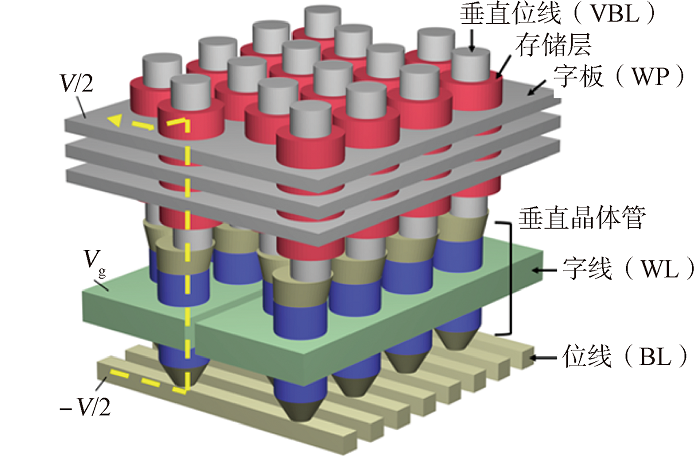
Huang K, Duan X, Feng J, et al. Vertical channel-all-around (CAA) IGZO FET under 50 nm CD with high read current of 32.8 μA/μm (Vth 1V), well-performed thermal stability up to 120 ℃ for low latency, high-density 2T0C 3D DRAM application[C]// 2022 IEEE Symposium on VLSI Technology and Circuits. Piscata-way: IEEE Press, 2022, doi: 10.1109/VLSITechnology-andcir46769.2022.9830271.
DOI |
| [35] |
Park K T, Nam S, Kim D, et al. Three-dimensional 128 Gb MLC vertical NAND flash memory with 24-WL stacked layers and 50 MB/s high-speed programming[J]. IEEE Journal of Solid-State Circuits, 2014, 50(1): 204-213.
DOI URL |
| [36] |
Jeong W, Im J, Kim D H, et al. A 128 Gb 3 b/cell V-NAND flash memory with 1 Gb/s I/O rate[J]. IEEE Journal of Solid-State Circuits, 2015, 51(1): 204-212.
DOI URL |
| [37] |
Kang D, Jeong W, Kim C, et al. 256 Gb 3 b/cell V-NAND flash memory with 48 stacked WL layers[J]. IEEE Journal of Solid-State Circuits, 2016, 52(1): 210-217.
DOI URL |
| [38] |
Kim C, Kim D H, Jeong W, et al. A 512-Gb 3-b/cell 64-stacked WL 3-D-NAND flash memory[J]. IEEE Journal of Solid-State Circuits, 2017, 53(1): 124-133.
DOI URL |
| [39] | Maejima H, Kanda K, Fujimura S, et al. A 512 Gb 3 b/cell 3D flash memory on a 96-word-line-layer technology[C]// 2018 IEEE International Solid-State Circuits Conference (ISSCC). Piscataway:IEEE Press, 2018: 336-338. |
| [40] | Siau C, Kim K H, Lee S, et al. 13.5 A 512 Gb 3-bit/cell 3D flash memory on 128-wordline-layer with 132 MB/s write performance featuring circuit-under-array technology[C]// 2019 IEEE International Solid-State Circuits Con-ference (ISSCC). Piscataway: IEEE Press, 2019, 218-220. |
| [41] | Park J W, Kim D, Ok S, et al. 30.1 A 176-stacked 512 Gb 3 b/cell 3D-NAND flash with 10.8 Gb/mm2 density with a peripheral circuit under cell array architecture[C]// 2021 IEEE International Solid-State Circuits Conference (ISSCC). Piscataway: IEEE Press, 2021, 64: 422-423. |
| [42] | Micron. 176 layers of innovation[EB/OL].[2022-07-23]. https://www.micron.com/products/nand-flash/176-layer-nand. |
| [43] |
Parat K, Dennison C. A floating gate based 3D NAND technology with CMOS under array[C]// 2015 IEEE International Electron Devices Meeting (IEDM). Piscataway: IEEE Press, 2015, doi: 10.1109/IEDM.2015.7409618.
DOI |
| [44] |
Kau D C, Tang S, Karpov I V, et al. A stackable cross point phase change memory[C]// 2009 IEEE International Electron Devices Meeting (IEDM). Piscataway: IEEE Press, 2009, doi: 10.1109/IEDM.2009.5424263.
DOI |
| [45] |
Huai Y, Albert F, Nguyen P, et al. Observation of spin-transfer switching in deep submicron-sized and low-resistance magnetic tunnel junctions[J]. Applied Physics Letters, 2004, 84(16): 3118-3120.
DOI URL |
| [46] | Klostermann U K, Angerbauer M, Gruning U, et al. A perpendicular spin torque switching based MRAM for the 28 nm technology node[C]// 2007 IEEE International Electron Devices Meeting. Piscataway: IEEE Press, 2007: 187-190. |
| [47] |
Miron I M, Garello K, Gaudin G, et al. Perpendicular switching of a single ferromagnetic layer induced by in-plane current injection[J]. Nature, 2011, 476(7359): 189-193.
DOI URL |
| [48] | Mahajan R, Sankman R, Patel N, et al. Embedded multi-die interconnect bridge (EMIB)—A high density, high bandwidth packaging interconnect[C]// 2016 IEEE 66th Electronic Components and Technology Conference (ECTC). Piscataway:IEEE Press, 2016: 557-565. |
| [49] | Jun H, Nam S, Jin H, et al. High-bandwidth memory (HBM) test challenges and solutions[J]. IEEE Design & Test, 2017, 34(1): 16-25. |
| [50] |
Kim K. The smallest engine transforming humanity: The past, present, and future[C]// 2021 IEEE International Electron Devices Meeting (IEDM). Piscataway: IEEE Press, 2022, doi: 10.1109/IEDM19574.2021.9720583.
DOI |
| [51] |
Jun H, Cho J, Lee K, et al. HBM (high bandwidth memory) DRAM technology and architecture[C]// 2017 IEEE International Memory Workshop (IMW). Piscataway: IEEE Press, 2017, doi: 10.1109/IMW.2017.7939084.
DOI |
| [52] |
Duan X, Huang K, Feng J, et al. Novel vertical channel-all-around (CAA) IGZO FETs for 2T0C DRAM with high density beyond 4 F2 by monolithic stacking[C]// 2021 IEEE International Electron Devices Meeting (IEDM). Piscataway: IEEE Press, 2021, doi: 10.1109/IEDM19574.2021.9720682.
DOI |
| [53] |
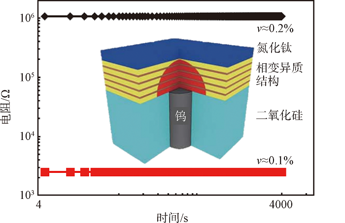
Ding K, Wang J, Zhou Y, et al. Phase-change heterostructure enables ultralow noise and drift for memory operation[J]. Science, 2019, 366(6462): 210-215.
DOI PMID |
| [54] |
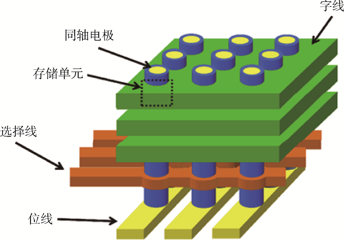
Yoo S, Kim D, Koo Y M, et al. Structural and device considerations for vertical cross point memory with single-stack memory toward CXL memory beyond 1x nm 3DXP[C]// 2022 IEEE International Memory Workshop (IMW). Piscataway: IEEE Press, 2022, doi: 10.1109/IMW52921.2022.9779247.
DOI |
| [55] |
Ali T, Olivo R, Kerdilès S, et al. Study of nanosecond laser annealing on silicon doped hafnium oxide film crystallization and capacitor reliability[C]// 2022 IEEE International Memory Workshop (IMW). Piscataway: IEEE Press, 2022, doi: 10.1109/IMW52921.2022.9779281.
DOI |
| [56] |
Florent K, Lavizzari S, Di Piazza L, et al. First demonstration of vertically stacked ferroelectric Al doped HfO2 devices for NAND applications[C]// 2017 Symposium on VLSI Technology. Piscataway: IEEE Press, 2017, doi: 10.23919/VLSIT.2017.7998162.
DOI |
| [57] | Yu S, Deng Y, Gao B, et al. Design guidelines for 3D RRAM cross-point architecture[C]// 2014 IEEE International Symposium on Circuits and Systems (ISCAS). Piscataway:IEEE Press, 2014: 421-424. |
| [58] |
Bocquet M, Hirztlin T, Klein J O, et al. In-memory and error-immune differential RRAM implementation of binarized deep neural networks[C]// 2018 IEEE International Electron Devices Meeting (IEDM). Piscataway: IEEE Press, 2018, doi: 10.1109/IEDM.2018.8614639.
DOI |
| [59] | Safranski C, Hu G, Sun J Z, et al., Reliable sub-nano-second MRAM with double spin-torque magnetic tunnel junctions[C]//2022 IEEE Symposium on VLSI Technology and Circuits (VLSI Technology and Circuits). Piscataway: IEEE Press, 2022: 288-289. |
| [60] |
Min M, Kadivar S. Accelerating innovations in the new era of HPC, 5G and networking with advanced 3D packaging technologies[C]// 2020 International Wafer Level Packaging Conference (IWLPC). Piscataway: IEEE Pressg, 2020, doi: 10.23919/IWLPC52010.2020.9375855.
DOI |
| [61] |
Niu D, Li S, Wang Y, et al. 184 QPS/W 64 Mb/mm2 3D logic-to-DRAM hybrid bonding with process-near-memory engine for recommendation system[C]// 2022 IEEE International Solid-State Circuits Conference (ISSCC). Piscataway: IEEE Press, 2022, doi: 10.1109/ISSCC42614.2022.9731694.
DOI |
| [62] | Park J. This is not your fathers advanced semiconductor packaging…An EDA perspective[R/OL]. [2022-07-23]. https://www.cadence.com/content/dam/cadence-www/global/en_US/documents/tools/ic-package-design-analysis/imaps-dev-pack-20-eda-perspective.pdf. |
| [63] | Knickerbocker J U, Andry P S, Dang B, et al. 3D silicon integration[C]// 2008 58th Electronic Components and Technology Conference. Piscataway: IEEE Press, 2008: 538-543. |
| [64] |
Knickerbocker J U, Andry P S, Dang B, et al. Three-dimensional silicon integration[J]. IBM Journal of Research and Development, 2008, 52(6): 553-569.
DOI URL |
| [65] | Thonnart Y, Bernabé S, Charbonnier J, et al. POPSTAR: A robust modular optical NoC architecture for chiplet-based 3D integrated systems[C]// 2020 Design, Automation & Test in Europe Conference & Exhibition (DATE). Piscataway:IEEE Press, 2020: 1456-1461. |
| [66] | Cerebras System. 2019 hot chips 32 symposium (HCS)[EB/OL].[2022-07-23]. https://venturebeat.com/2019/08/19/cerebras-systems-unveils-a-record-1-2-trillion-transistor-chip-for-ai/amp/?from=timeline. |
| [1] | WANG Wenwu, LUO Jun, WANG Xiaolei, XU Hao. Status of Global Research and Development Cooperation in Integrated Circuits and Its Inspiration [J]. Science and Technology Foresight, 2022, 1(3): 10-19. |
| [2] | ZHAO Jinrong, WEI Gang, HOU Jue, CAO Yongyou, DONG Jinwei, LU Xisheng, SUN Wei. Current Situation and Development Trend of Core Process Equipment Technologies for Integrated Circuit [J]. Science and Technology Foresight, 2022, 1(3): 61-72. |
| [3] | LIU Weiping, WANG Zongyuan. Development Status and Trend of EDA and IP Core Industries [J]. Science and Technology Foresight, 2022, 1(3): 90-100. |
| [4] | DONG Junchen, ZHANG Xing. Prospects of Advanced Integrated Circuit Technologies in Post-Moore Era [J]. Science and Technology Foresight, 2022, 1(3): 42-51. |
| Viewed | ||||||
|
Full text |
|
|||||
|
Abstract |
|
|||||


京公网安备 11010802038735号

