| [1] |
李冰. 集成电路制造用光刻胶发展现状及挑战[J]. 精细与专用化学品, 2021, 29(2): 1-5.
|
| [2] |
Matsuyama T, Ohmura Y, Williamson D M. The lithographic lens: Its history and evolution[C]// Proceedings of SPIE. Bellingham: SPIE, 2006, 6154: 24-37.
|
| [3] |
Mark N. International roadmap for devices and systems lithography roadmap[J]. Journal of Micro/Nanopatterning, Materials, and Metrology, 2021, doi: 10.1117/1.JMM.20.4.044601.
DOI
|
| [4] |
李艳丽, 刘显和, 伍强. 先进光刻技术的发展历程与最新进展[J]. 激光与光电子学进展, 2022, 59(9): 76-92.
|
| [5] |
Fedor G P, Andres T. Advanced multi-patterning and hybrid lithography techniques[M]. Piscataway: IEEE Press, 2016.
|
| [6] |
Finders M, Dusa M, Vleeming B, et al. Double patterning lithography for 32 nm: Critical dimensions uniformity and overlay control considerations[J]. Journal of Micro/Nanolithography, MEMS, and MOEMS, 2009, doi: 10.1117/1.3079349.
DOI
|
| [7] |
Panneerchelvam P, Huard C, Agarwal A, et al. Trilayer hard mark lithography and etch for BEOL manufacturing[C]// Proceedings of SPIE. Bellingham: SPIE, 2022, doi: 10.1117/12.2614095.
DOI
|
| [8] |
Oyama K, Nishimura E, Kushibiki M, et al. The important challenge to extend spacer DP process towards 22 nm and beyond[C]// Proceedings of SPIE. Bellingham: SPIE, 2010, doi: 10.1117/12.845970.
DOI
|
| [9] |
Jung W Y, Kim C D, Eom J D, et al. Patterning with spacer for expanding the resolution limit of current lithography tool[C]// Proceedings of SPIE. Bellingham: SPIE, 2006, doi: 10.1117/12.650991.
DOI
|
| [10] |
李冰, 马洁, 刁翠梅, 等. 光刻胶材料发展状况及下一代光刻技术对图形化材料的挑战[J]. 新材料产业, 2018, (12): 43-47.
|
| [11] |
Allen R D, Wallraff G, Hinsberg W, et al. High performance acrylic polymers for chemically amplified photoresist applications[J]. Journal of Vacuum Science & Technology B: Microelectronics and Nanometer Structures, 1991, doi: 10.1116/1.585341.
DOI
|
| [12] |
Ito H. Chemical amplification resists: History and development within IBM[J]. IBM Journal of Research and Development, 1997, 41(1-2): 119-130.
|
| [13] |
Goldfarb D L. Evolution of patterning materials towards the Moore,s law 2.0 era[J]. Japanese Journal of Applied Physics, 2022, doi: 10.35848/1347-4065/ac5534.
DOI
|
| [14] |
Higgins C D, Szmanda C R, Antohe A, et al. Resolution, line-edge roughness, sensitivity tradeoff, and quantum yield of high photo acid generator resists for extreme ultraviolet lithography[J]. Japanese Journal of Applied Physics, 2011, doi: 10.1143/JJAP.50.036504.
DOI
|
| [15] |
Matsunaga K, Oori T, Kato H, et al. LWR reduction in low-k1 ArF-immersion lithography[C]// Proceedings of SPIE. Bellingham: SPIE, 2008, doi: 10.1117/12.771922.
DOI
|
| [16] |
Han Q H, Meng X Y, Huang J Y, et al. The critical role of the plasma-based post litho treatment[J]. ECS Transactions, 2014, 60(1): 355-360.
DOI
URL
|
| [17] |
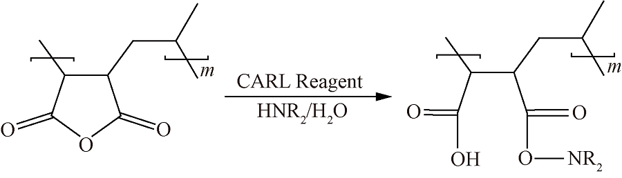
Sebald M, Seize R, Leuschner R, et al. Chemical amplification of resist lines (CARL)[J]. Microelectronic Engineering, 1990, 11(1-4): 531-534.
DOI
URL
|
| [18] |
Toyoshima T, Ishibashi T, Yasuda N, et al. Below 100-nm hole pattern formation using resolution enhancement lithography assisted by chemical shrink (RELACS)[J]. Journal of Photopolymer Science and Technology, 2002, 15(3): 377-278.
DOI
URL
|
| [19] |
Terai M, Kumada T, Ishibashi T, et al. Newly developed resolution enhancement lithography assisted by chemical shrink process and materials for next-generation devices[J]. Japanese Journal of Applied Physics, 2006, 45(6s): 5354-5358.
DOI
URL
|
| [20] |
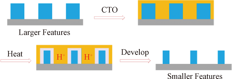
Liu C, Rowell K, Joesten L, et al. Chemical trimming overcoat: An enhancing composition and process for 193 nm lithography[C]// Proceedings of SPIE. Bellingham: SPIE, 2016, doi: 10.1117/12.2219688.
DOI
|
| [21] |
Uzodinma O. Chemistry and Lithography[M]. Bellingham: SPIE Press, 2010.
|
| [22] |
Uzodinma O. Materials and methods for sub-lithographic patterning of contact,via, and trench structures in integrated circuit devices: US, 6767693[P]. 2004-07-27.
|
| [23] |
Burns S, Burkhardt M, Goldfarb D, et al. Trilayer development for 193 nm immersion lithography[J]. Journal of Photopolymer Science and Technology, 2007, 20(5): 679-686.
DOI
URL
|
| [24] |
Burns S, Pfeiffer D, Mahorowala A, et al. Silicon containing polymer in applications for 193 nm high NA lithography processes[C]// Proceedings of SPIE. Bellingham: SPIE, 2006, doi: 10.1117/12.657197.
DOI
|
| [25] |
Coughlin Associates, Inc. Changxin memory technologies: China,s rising DRAM manufacture[R/OL]. (2021-06-05)[2022-08-01].https://tom-coughlin.com/wp-content/uploads/2021/06/First-CXMT-White-Paper-20210605-final.pdf.
|
 ), SUN Jia, CHEN Cindy Xin(