| [1] |
Zhang G Q, Graef M, van Roosmalen F. The rationale and paradigm of “more than Moore”[C]// 56th Electronic Components and Technology Conference 2006. Piscataway: IEEE Press, 2006, doi: 10.1109/ECTC.2006.1645639.
DOI
|
| [2] |
Bishop M D, Wong H S P, Mitra S, et al. Monolithic 3-D integration[J]. IEEE Micro, 2019, 39(6): 16-27.
DOI
|
| [3] |
Gholami A. AI and memory wall[EB/OL]. (2021-05-29)[2022-06-10]. https://medium.com/riselab/ai-and-memory-wall-2cb4265cb0b8.
|
| [4] |
Su L T, Naffziger S, Papermaster M. Multi-chip technologies to unleash computing performance gains over the next decade[C]// IEEE International Electron Devices Meeting (IEDM). Piscataway: IEEE Press, 2018, doi: 10.1109/IEDM.2017.8268306.
DOI
|
| [5] |
Mahajan R, Penmecha B, Radhakrishman K. Advanced packaging architectures for heterogeneous integration[C]. MechSE Seminars. 190 Engineering Sciences Building, 2021.
|
| [6] |
Tummala R R. Moore,s law meets its match (system-on-package)[J]. IEEE Spectrum, 2006, 43(6): 44-49.
|
| [7] |
Yeric G. Three dimensions in 3DIC-Part I[EB/OL].(2018-04-02)[2022-08-10]. https://community.arm.com/arm-research/b/articles/posts/three-dimensions-in-3dic-part-1.
|
| [8] |
Su L. Cost per yielded mm2 for a 250 mm2 die[C]// IEEE International Electron Devices Meeting (IEDM). San Francisco:2017.
|
| [9] |
Gomes W, Koker A, Stover P, et al. Ponte Vecchio: A multi-tile 3D stacked processor for exascale computing[C]// IEEE International Solid-State Circuits Conference (ISSCC). Piscataway: IEEE Press, 2022, doi: 10.1109/ISSCC42614.2022.9731673.
DOI
|
| [10] |
Mujtaba H. AMD discloses its multi-layer chiplet design era, starting with Zen 3 with 3D stacked V-cache technology[EB/OL].(2021-08-22)[2022-05-10]. https://wccftech.com/amd-discloses-multi-layer-chip-design-era-starting-with-zen-3-with-3d-stacked-v-cache-technology/.
|
| [11] |
Vivet P, Guthmulle E, Thonnart Y, et al. IntAct: A 96-core processor with six chiplets 3D-stacked on an active interposer with distributed interconnects and integrated power management[J]. IEEE Journal of Solid-State Circuits, 2021, 56(1): 79-97.
DOI
URL
|
| [12] |
Hruska J. TSMC announces its first 16 nm FinFET networking chip: 32-core ARM Cortex-A57[EB/OL].(2014-09-26)[2022-05-10]. https://www.extremetech.com/computing/190941-tsmc-announces-its-first-16nm-finfet-net-working-chip-32-core-arm-cortex-a57.
|
| [13] |
William S. Semiconductive wafer and method of making the same: US, 3044909[P]. 1962-07-17.
|
| [14] |
Huang P K, Lu C Y, Wei W H, et al. Wafer level system integration of the fifth generation CoWoS®-S with high performance Si interposer at 2500 mm2[C]// 2021 IEEE 71st Electronic Components and Technology Conference. Piscataway: IEEE Press, 2021, doi: 10.1109/ECTC32696.2021.00028.
DOI
|
| [15] |
Chaware R, Nagarajan K, Ramalingam S. Assembly and reliability challenges in 3D integration of 28 nm FPGA die on a large high density 65 nm passive interposer[C]// 2012 IEEE 62nd Electronic Components and Technology Conference. Piscataway: IEEE Press, 2012, doi: 10.1109/ECTC.2012.6248841.
DOI
|
| [16] |
Banijamali B, Ramalingam S, Liu H, et al. Outstanding and innovative reliability study of 3D TSV interposer and fine pitch solder micro-bumps[C]// 2012 IEEE 62nd Electronic Components and Technology Conference. Piscataway: IEEE Press, 2012, doi: 10.1109/ECTC.2012.6248847.
DOI
|
| [17] |
Balaban S. NVIDIA A100 GPU-deep learning benchmark estimates[EB/OL]. (2020-05-22)[2022-05-10]. https://lambdalabs.com/blog/nvidia-a100-gpu-deep-learning-bench-marks-and-architectural-overview/.
|
| [18] |
Coudrain P, Charbonnier J, Garnier A, et al. Active interposer technology for chiplet-based advanced 3D system architectures[C]// 2019 IEEE 69th Electronic Components and Technology Conference (ECTC). Piscataway: IEEE Press, 2019, doi: 10.1109/ECTC.2019.00092.
DOI
|
| [19] |
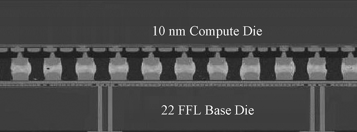
Gomes W, Khushu S, Ingerly D B, et al. 8.1 lakefield and mobility compute: A 3D stacked 10 nm and 22 FFL hybrid processor system in 12×12 mm2, 1 mm package-on-package[C]//2020 IEEE International Solid-State Circuits Conference (ISSCC). Piscataway: IEEE Press, 2020, doi: 10.1109/ISSCC19947.2020.9062957.
DOI
|
| [20] |
Jun H, Cho J, Lee K, et al. HBM (High Bandwidth Memory) DRAM technology and architecture[C]// 2017 IEEE International Memory Workshop (IMW). Piscata-way: IEEE Press, 2017, doi: 10.1109/IMW.2017.7939084.
DOI
|
| [21] |
Chun S R, Kuo T H, Yi H, et al. InFO_SoW (System-on-Wafer) for high performance computing[C]// 2020 IEEE 70th Electronic Components and Technology Conference (ECTC). Piscataway: IEEE Press, 2020, doi: 10.1109/ECTC32862.2020.00013.
DOI
|
| [22] |
Tesla AI Day 2021 Review—Part 3: DojoProject. Tesla,s new supercomputer[EB/OL]. (2021-10-11)[2022-05-10]. https://towardsdatascience.com/tesla-ai-day-2021-review-part-3-project-dojo-teslas-new-supercomputer-715d102dbb29.
|
| [23] |
Mahajan R, Sane S. Microelectronic package containing silicon patches for high density interconnects: US, 8064.224 B2[P]. 2011-11-22.
|
| [24] |
Braunisch H, Aleksov A, Lotz S, et. al. High-speed performance of silicon bridge die-to-die interconnects[C]// 2011 IEEE 20th Conference on Electrical Performance of Electronic Packaging and Systems. Piscataway: IEEE Press, 2011, doi: 10.1109/EPEPS.2011.6100196.
DOI
|
| [25] |
Starkston D M R, Guzek J S, Chiu C P. Localized high density substrate routing: US, 9136236, B2[P]. 2015-09-15.
|
| [26] |
Mahajan R, Sankman R, Patel N, et al. Embedded multi-die interconnect bridge (EMIB): A high density, high bandwidth packaging interconnect[C]// 2016 IEEE 66th Electronic Components and Technology Conference (ECTC). Piscataway: IEEE Press, 2016, doi: 10.1109/ECTC.2016.201.
DOI
|
| [27] |
Mahajan R, Qian Z, Viswanath R S, et al. Embedded multidie interconnect bridge: A localized, high-density multichip packaging interconnect[J]. IEEE Transactions on Components, Packaging and Manufacturing Technology, 2019, 9(10): 1952-1962.
DOI
URL
|
 ), 侯峰泽(